
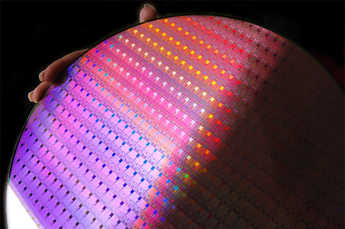
One of the interesting disclosures here at the IEEE International Electron Devices Meeting (IEDM) has been around new and upcoming process node technologies. Almost every session so far this week has covered 7nm, 5nm, and 3nm processes (as the industry calls them). What we didn’t expect to see disclosed was an extended roadmap of Intel’s upcoming manufacturing processes.
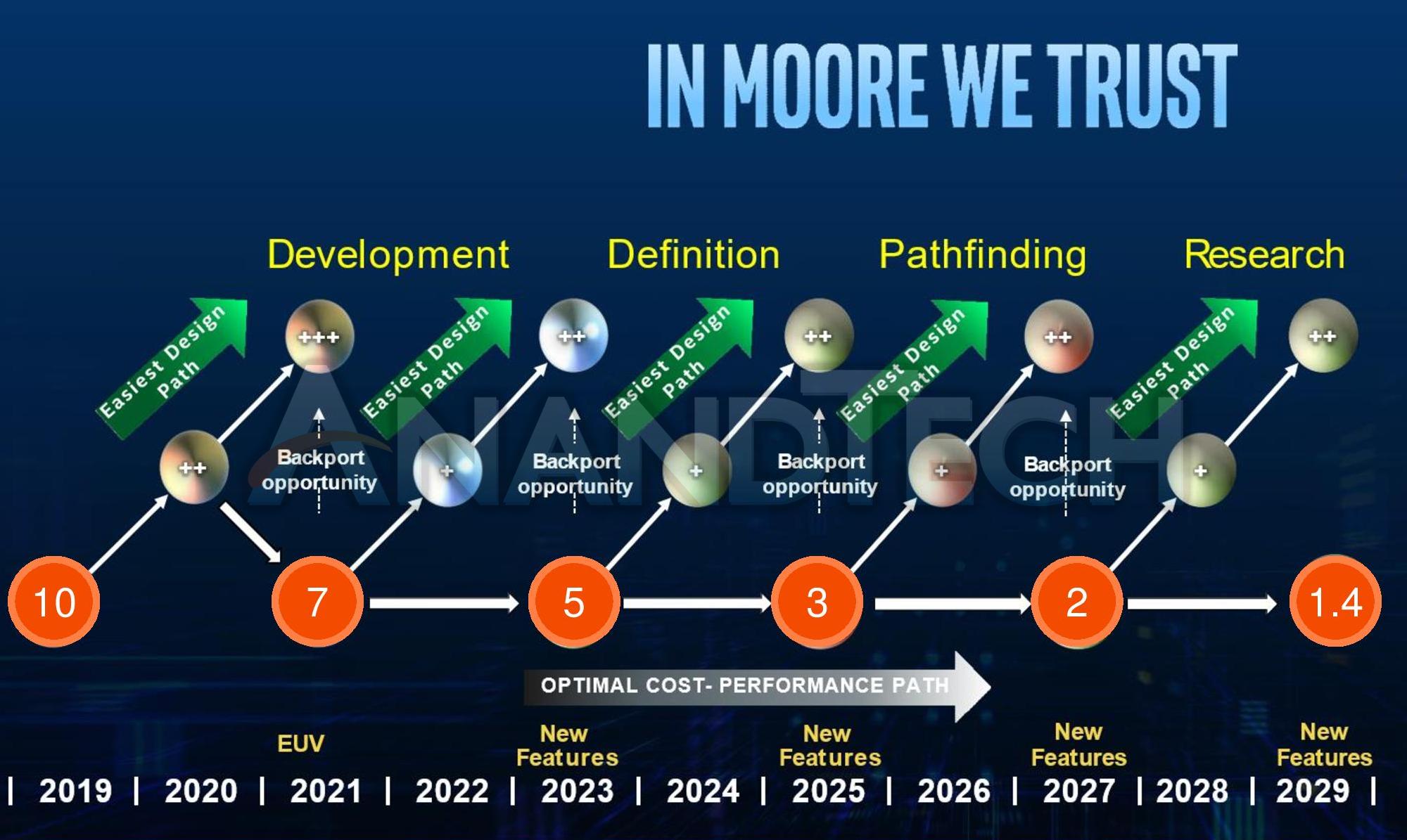
They say a slide is worth 1000 words. Here’s 1000 words on Intel’s future.
The talk which disclosed this data was actually one of the key talks of the IEDM conference through one of Intel’s close partners, who states that Intel themselves presented this slide at a lithography conference back in September. Here’s the slide.
So let’s go through some key areas.
1.4nm in 2029
Intel expects to be on 2 year cadence with its manufacturing process node technology, starting with 10nm in 2019 and moving to 7nm EUV in 2021, then 5nm in 2023, 3nm in 2025, 2nm in 2027, and 1.4 nm in 2029. This is the first mention on 1.4nm for Intel on any slide, so this confirms where Intel is going, and just for context, if that 1.4nm is indicative of any actual feature, would be the equivalent of 12 silicon atoms across.
It is perhaps worth noting that some of the talks at this year’s IEDM features dimensions on the order of 0.3nm with what are called ‘2D self-assembly’ materials, so something this low isn’t unheard of, but it is unheard of in silicon. Obviously there are many issues going that small that Intel (and its partners) will have to overcome.
+, ++, and Back Porting
Inbetween each process node, as Intel has stated before, there will be iterative + and ++ versions of each in order to extract performance from each process node. The only exception to this is 10nm, which is already on 10+, so we will see 10++ and 10+++ in 2020 and 2021 respectively. Intel believes they can do this on a yearly cadence, but also have overlapping teams to ensure that one full process node can overlap with another.
The interesting element to this slide is the mention of back porting. This is the ability for a chip to be designed with one process node in mind, but perhaps due to delays, can be remade on an older ‘++’ version of a process node in the same timeframe. Despite Intel stating that they are disaggregating chip design from process node technology, at some point there has to be a commitment to a process node in order to start the layouts in silicon. At that point the process node procedure is kind of locked, especially when it goes to mask creation.
In the slide, it shows that Intel is going to allow a workflow such that any first gen 7nm design could be back ported to 10+++, any first gen 5nm design could be back ported to 7++, then 3nm to 5++, 2nm to 3++, and so on. One can argue that this roadmap might not be so strict with the dates – we have seen Intel’s 10nm take a long time to bake, so expecting the company to move with a yearly cadence on + updates alongside a two-year cadence with main process technology nodes would appear to be a very optimistic and aggressive cadence strategy.
Note that this isn’t the first mention of back porting hardware designs when it comes to Intel. With the current delays to Intel’s 10nm process technology, it has been widely rumoured that some of Intel’s future CPU microarchitecture designs, originally designed with 10nm (or 10+, 10++) in mind might actually find a home on a 14nm process due to the success of that process node.
Development and Research
Normally with process node developments, there will be different teams working on each process node. This slide states that Intel is currently in development of its 10+++ optimizations as well as the 7nm family. The idea is that the ‘+’ updates are capturing the low hanging fruit from a design standpoint every generation, and the number represents a full node benefit. Interestingly we see Intel’s 7nm being based on 10++, whereas in the future Intel sees 5nm come from the base 7nm design, and 3nm coming from 5nm. There is no doubt that some of the optimizations that enter each +/++ update will filter into future designs as and when they are needed.
In this slide, we have Intel’s 5nm currently in the definition stage. At this IEDM conference there’s a lot of talk about 5nm, so some of those improvements (such as manufacturing, materials, consistency, etc.) will ultimately end up in Intel’s 5nm process depending on which design houses they partner with (historically Applied Materials). It is worth noting that 5nm is listed as a 2023 node, which is around the time that ASML will start selling its ‘High NA’ EUV machines to help with better path definition during the manufacturing process. I’m not sure if High NA will intercept at 5nm or 3nm, assuming this Intel roadmap has its dates correct and Intel is able to stick to it, but it is something to consider
Beyond 5nm, looking at 3nm/2nm/1.4nm, Intel is currently in the ‘path-finding’ mode. As always when looking this far out, Intel is considering new materials, new transistor designs, and such. At this IEDM conference we’re seeing a lot of talk of gate-all-around transistors, either as nano-sheets or nano-wires, so no doubt we’re going to see some of that as FinFET runs out of steam. TSMC is still using FinFETs for its 5nm process (Intel’s 7nm equivalent), so I wouldn’t be surprised if we see something like nano-sheets then nano-wires (or even hybrid designs) come into Intel’s manufacturing stack.
It’s worth also pointing out, based on the title of this slide, that Intel still believes in Moore’s Law. Just don’t ask how much it’ll cost.