

One of the interesting elements that came out of some of our discussions at the IEDM conference this year revolves around the present deployment of EUV. Currently only one company makes EUV tools, ASML, and the deployment of these to the various foundries that are on the leading edge has been a topic of some discussion here at the event, especially as we start talking about 7nm, 5nm, 3nm, and new generations of tools.
One of the interesting metrics that we’ve seen from ASML is the total number of 300mm wafers that have been enabled through EUV. Early adoption of EUV actually started all the way back in 2013, and it took until 2017 to push through over 1,000,000 wafers. In 2018 another 900,000 wafers were processed, and through 2019, with chips such as Huawei’s Kirin 990 5G, Qualcomm’s upcoming Snapdragon 700 series, and Samsung’s own EUV efforts, another 2.5 million wafers have been processed, showing an explosive CAGR of 95% since 2016.
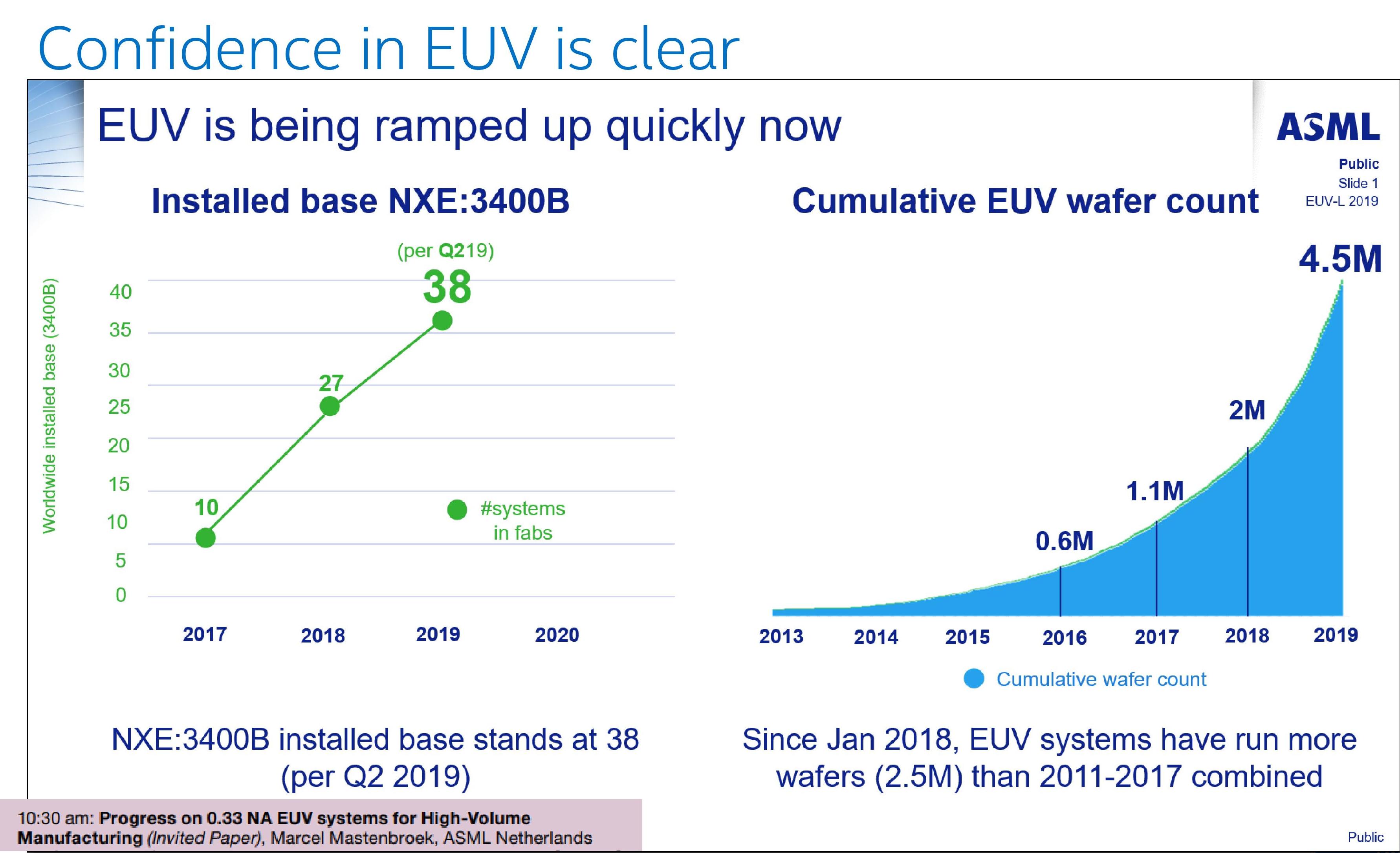
Along with that, ASML’s NXE:3400B Step and Scan machines have been at the heart of most of this EUV production. As the graph above shows, 38 machines were installed by Q2 2019, and through 2019 the B versions have been replaced with the NXE:3400C editions, which can process at peak 175 wafers per hour.
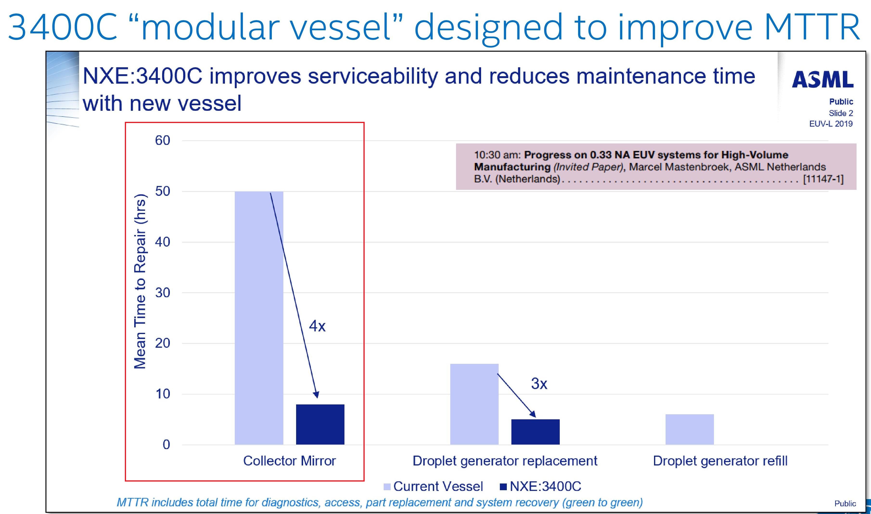
One of the advantages of the NXE:3400C models is the modularity in its design, meaning that a mirror defect should take only an 8-10 hour replacement, rather than take the machine out of action for a full 48 hours.
A note on EUV machine uptime is a key metric: 175 wafers per hour is fast for EUV, but that doesn’t matter much if the machine is being repaired for 2-3 days out of every week. To that end, Intel showed off a slide at a recent lithography conference to give some insight into their EUV uptime and downtime.

With 168 hours per week, in late 2018 Intel’s EUV machines (3400B) were running only half the week, with some weeks having 80-90% downtime. Moving into the middle of 2019, such as week 14, they’re showing up to a day of combined planned uptime/downtime, which still makes for 14-20% downtime. It’s worth noting that Intel has not yet sold silicon publicly using an EUV process, so this is still for calibration, testing, and development time. Intel is expected to introduce EUV into its leading performance processors with 7nm, which could be ready for risk production by 2021.
ASML is keen to promote its improvement in wafer throughput of its NXE machines, from a little over 10 wafers per hour in 2014 to 170-175 in 2019.

Beyond the NXE lines of machines will be the EXE:5000 series. What makes these machines different is that they are built for the equivalent of TSMC’s 3nm / Intel’s 5nm processes by using ‘High-NA’ technology, technically moving from 0.33 NA optics to 0.55 NA optics, which will help improve manufacturing features at smaller and smaller resolutions. It will be interesting to see if the speed of the High-NA EXE machines will be similar or better to the NXE machines. Based on ASML’s presentation, High-NA machines should be coming into the market by 2023, by which time EUV use should be extensive at the leading edge.
Related Reading
- EUV Demand is Up: EUV Device Manufacturer ASML Beats Sales Estimates
- ASML to Ship 30 EUV Scanners in 2019: Faster EUV Tools Coming
- ASML Ships Twinscan NXT:2000i Scanner for 7nm and 5nm DUV
- Intel’s Manufacturing Roadmap from 2019 to 2029: Back Porting, 7nm, 5nm, 3nm, 2nm, and 1.4 nm
- Samsung Announces Exynos 990: 7nm EUV, M5, G77, LPDDR5 Flagship SoC alongside Exynos 5123 5G Modem
- TSMC: N7+ EUV Process Technology in High Volume, 6nm (N6) Coming Soon
- Samsung Announces the Exynos 9825 SoC: First 7nm EUV Silicon Chip
- Samsung’s Aggressive EUV Plans: 6nm Production in H2, 5nm & 4nm On Track