
09:03PM EDT – The final presentation of Hot Chips 31 is from Microsoft, who will be lifting the lid of the silicon behind its HoloLens 2.0 product.
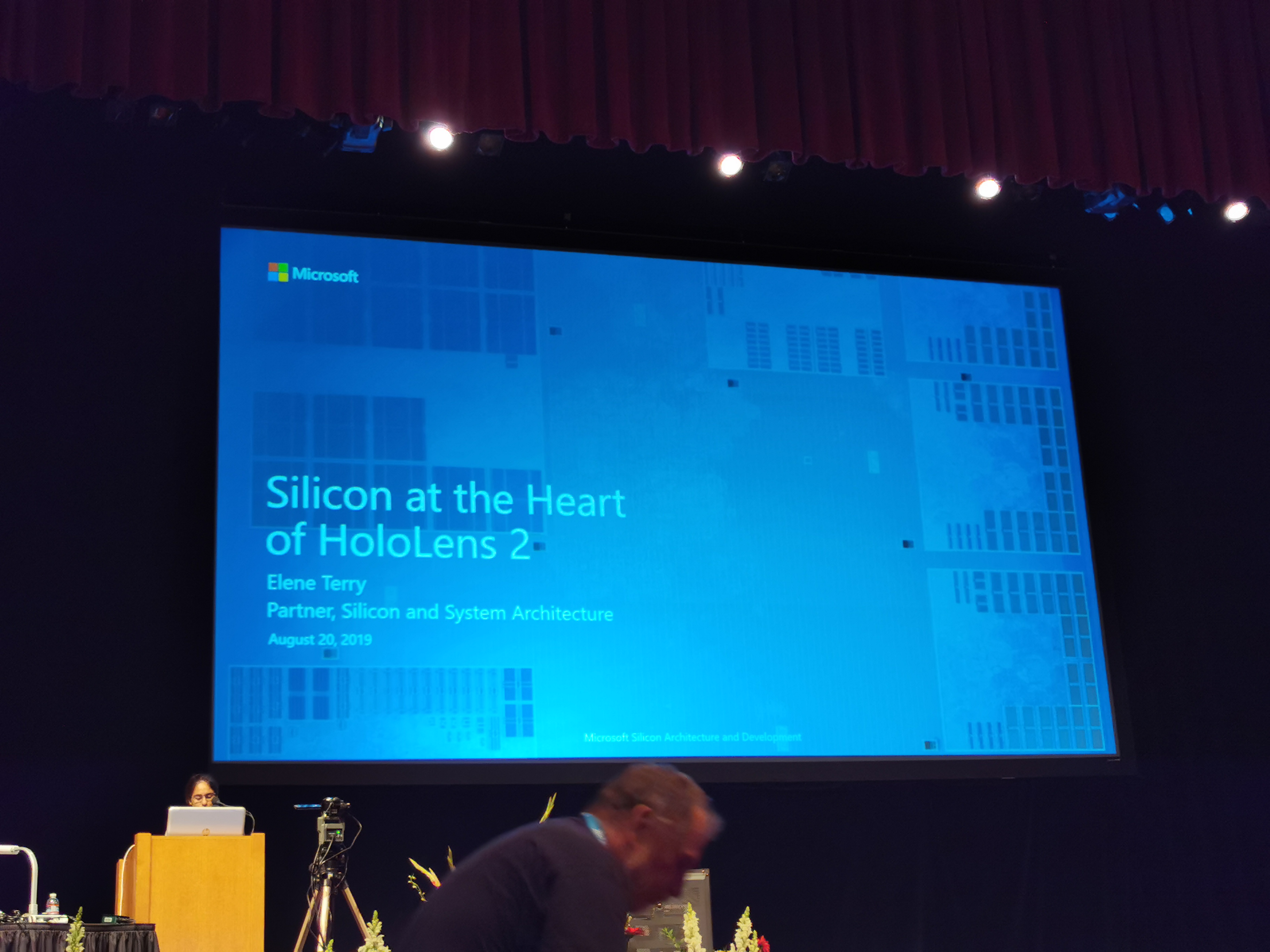
09:17PM EDT – Here we go
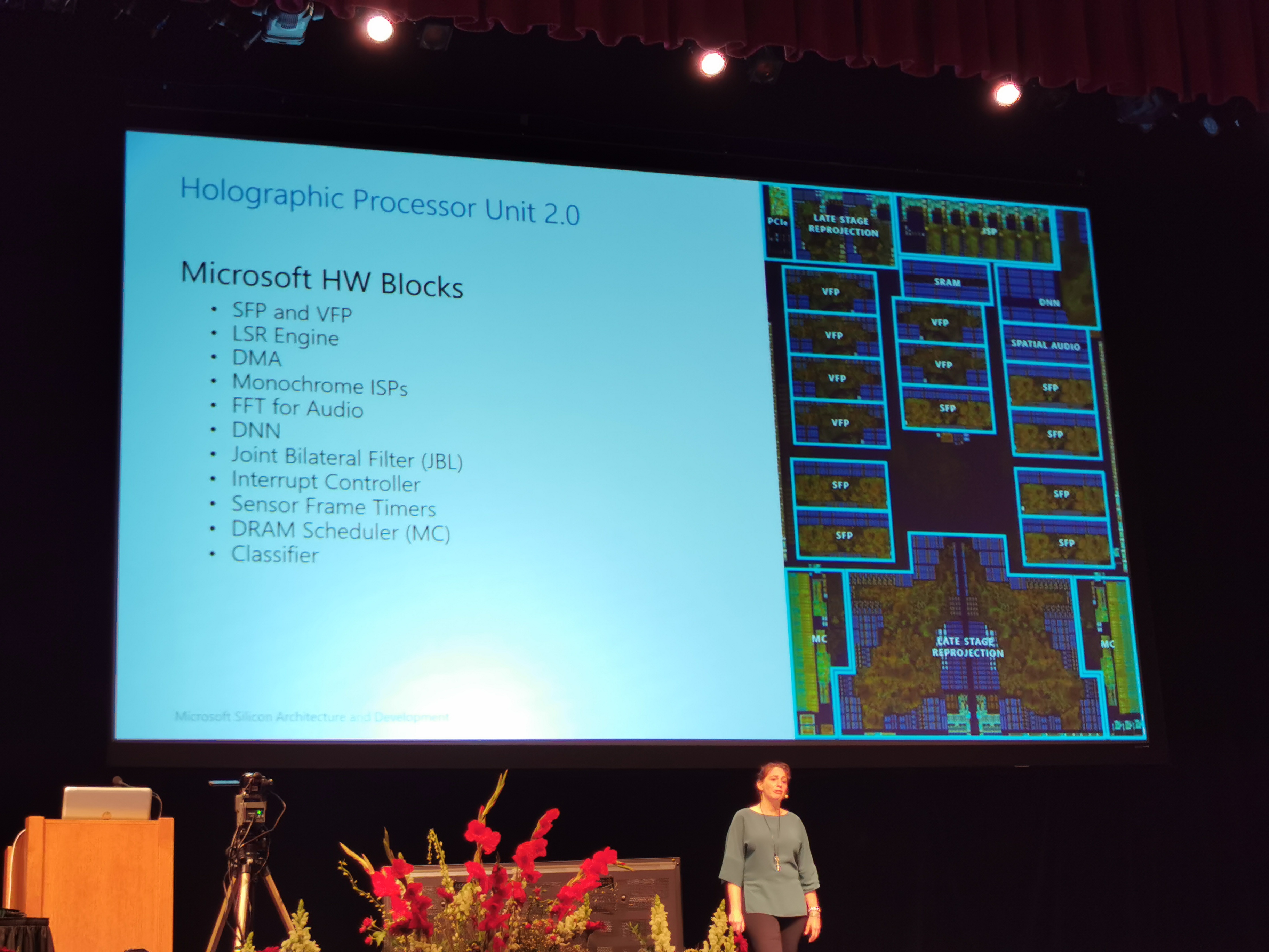
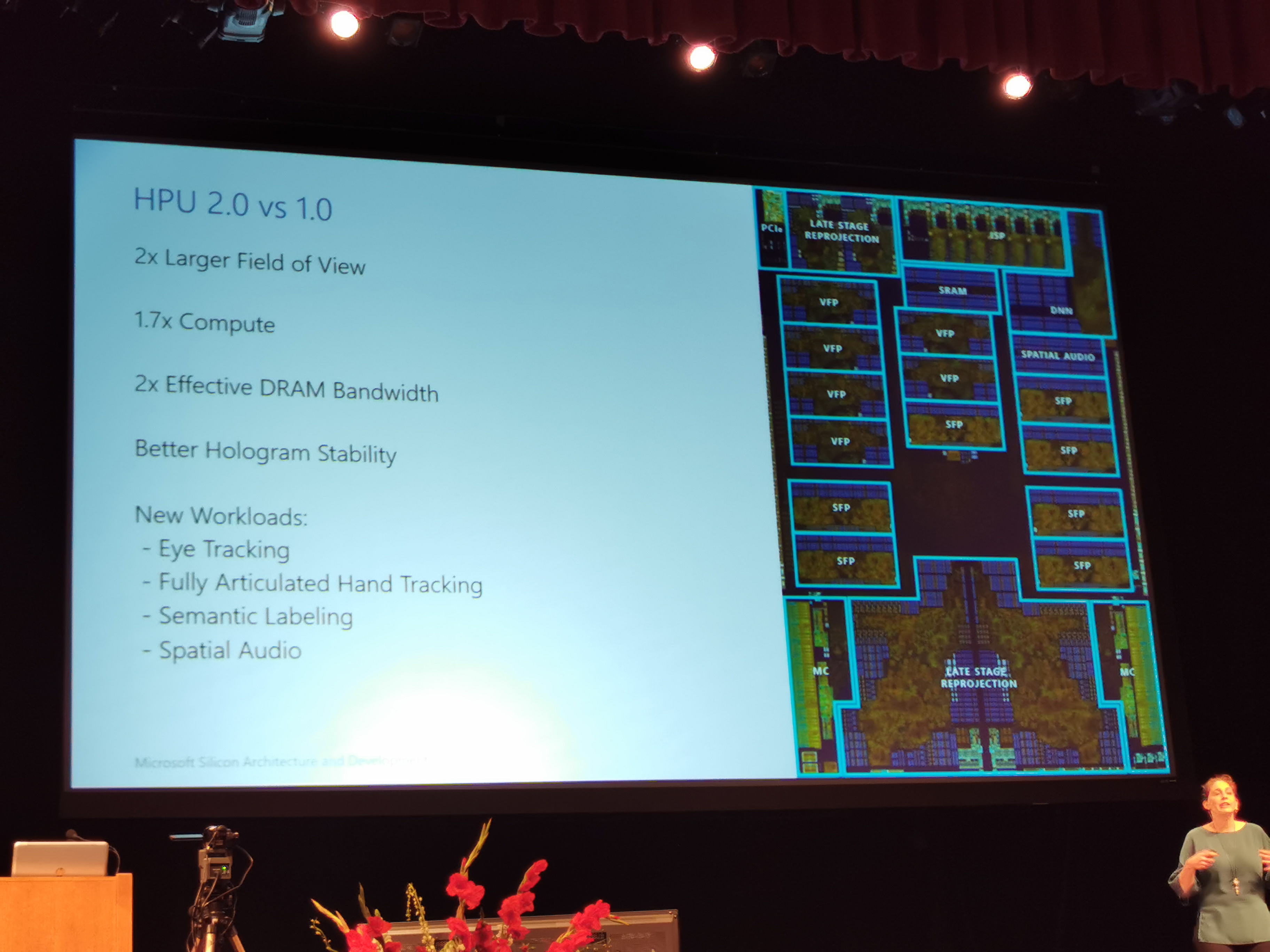
09:17PM EDT – HPU 2.0
09:18PM EDT – Holographic processor
09:18PM EDT – Custom silicon, obviously
09:19PM EDT – This speaker has been trained. There are purposeful pauses when she lists stuff
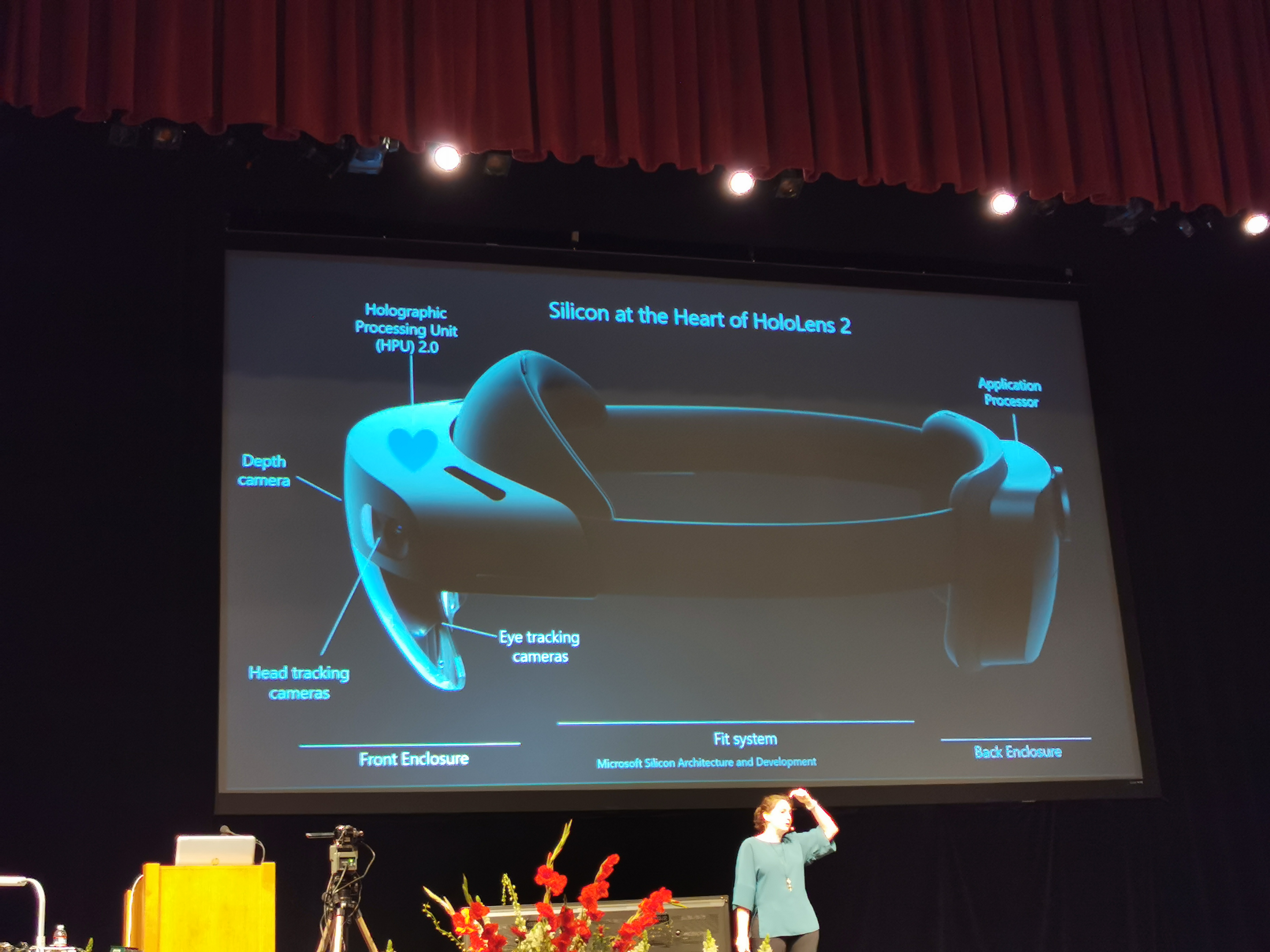
09:20PM EDT – Application processor runs the app, and the HPU modifies the rendered image and sends to the display
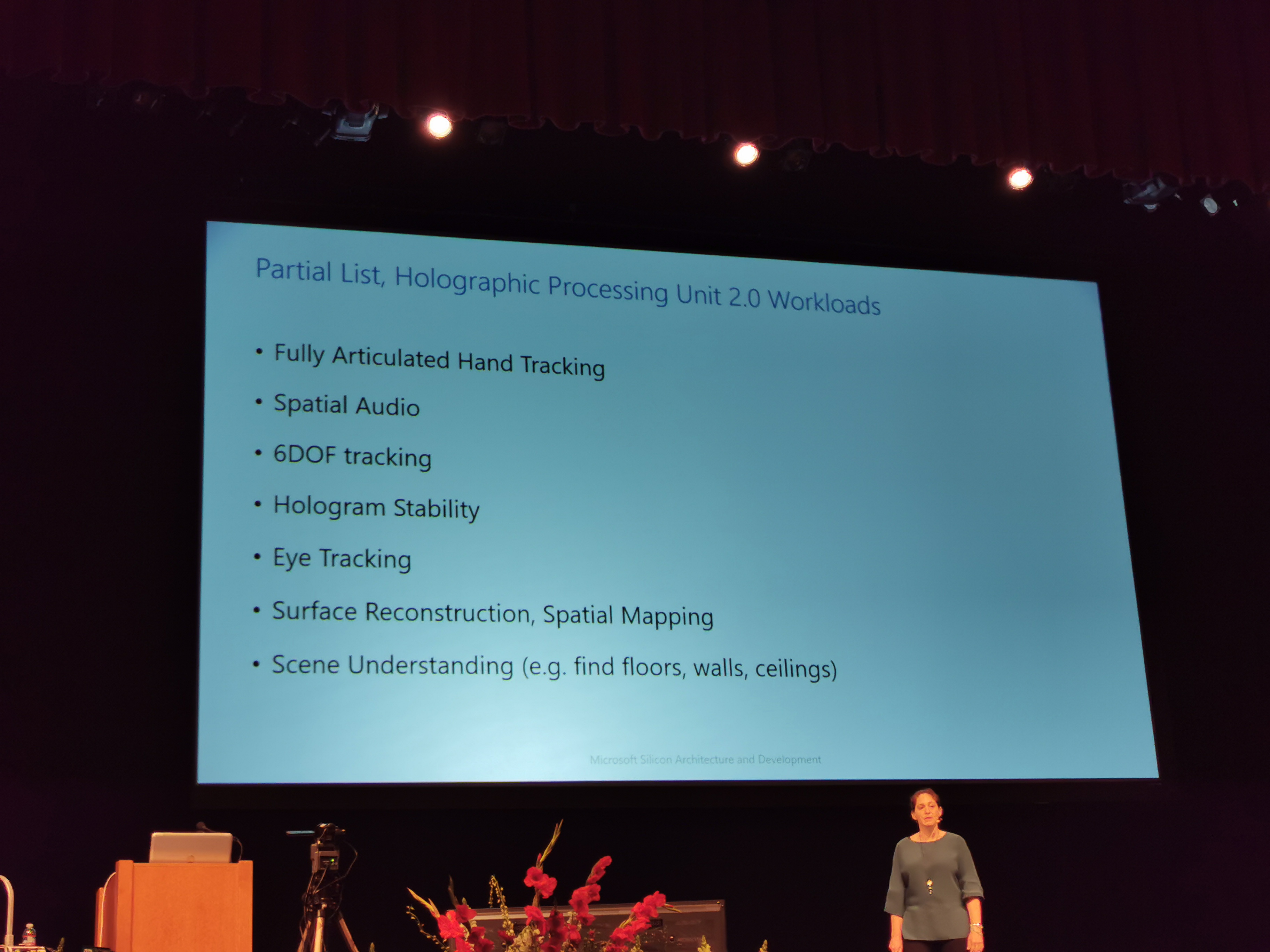
09:20PM EDT – HPU works on specific workloads
09:21PM EDT – Takes the visual cues and allows the HPU to track where the hands are at all times
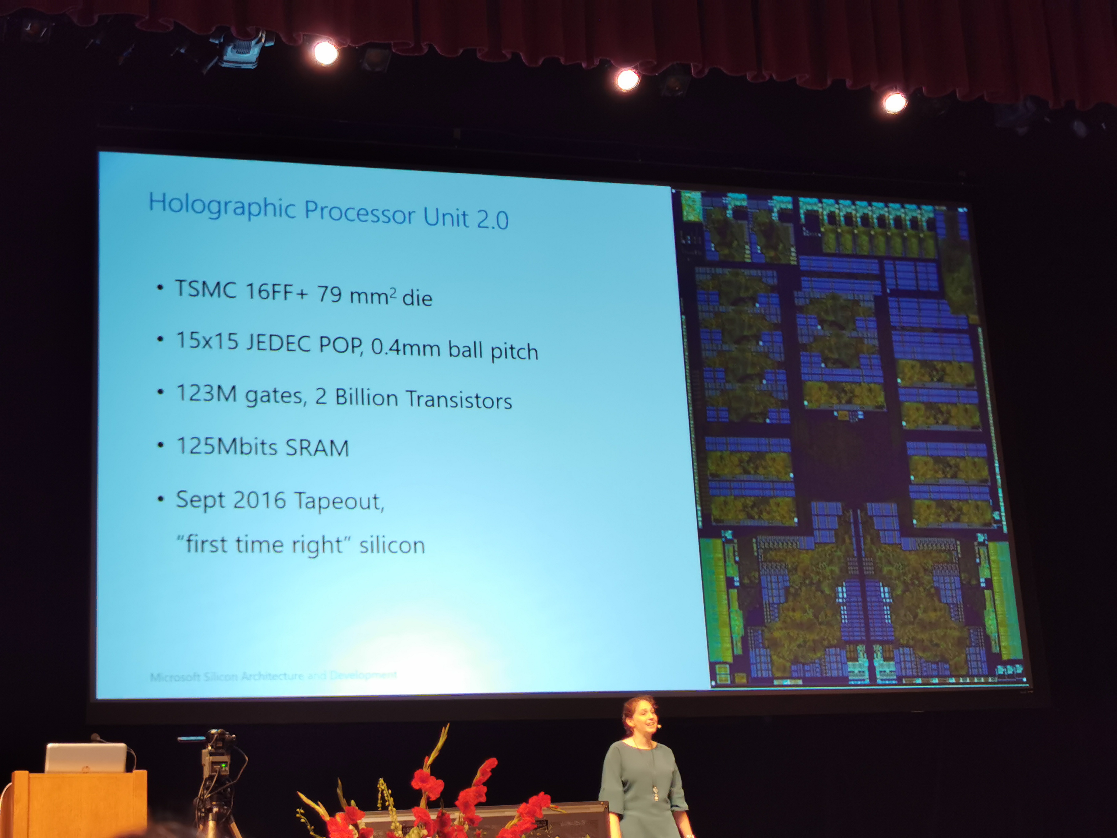
09:21PM EDT – 79mm2 on TSMC 16FF+
09:21PM EDT – 123M gates, 2B transistors
09:22PM EDT – 2016 Tapeout
09:22PM EDT – 125 Mb of SRAM
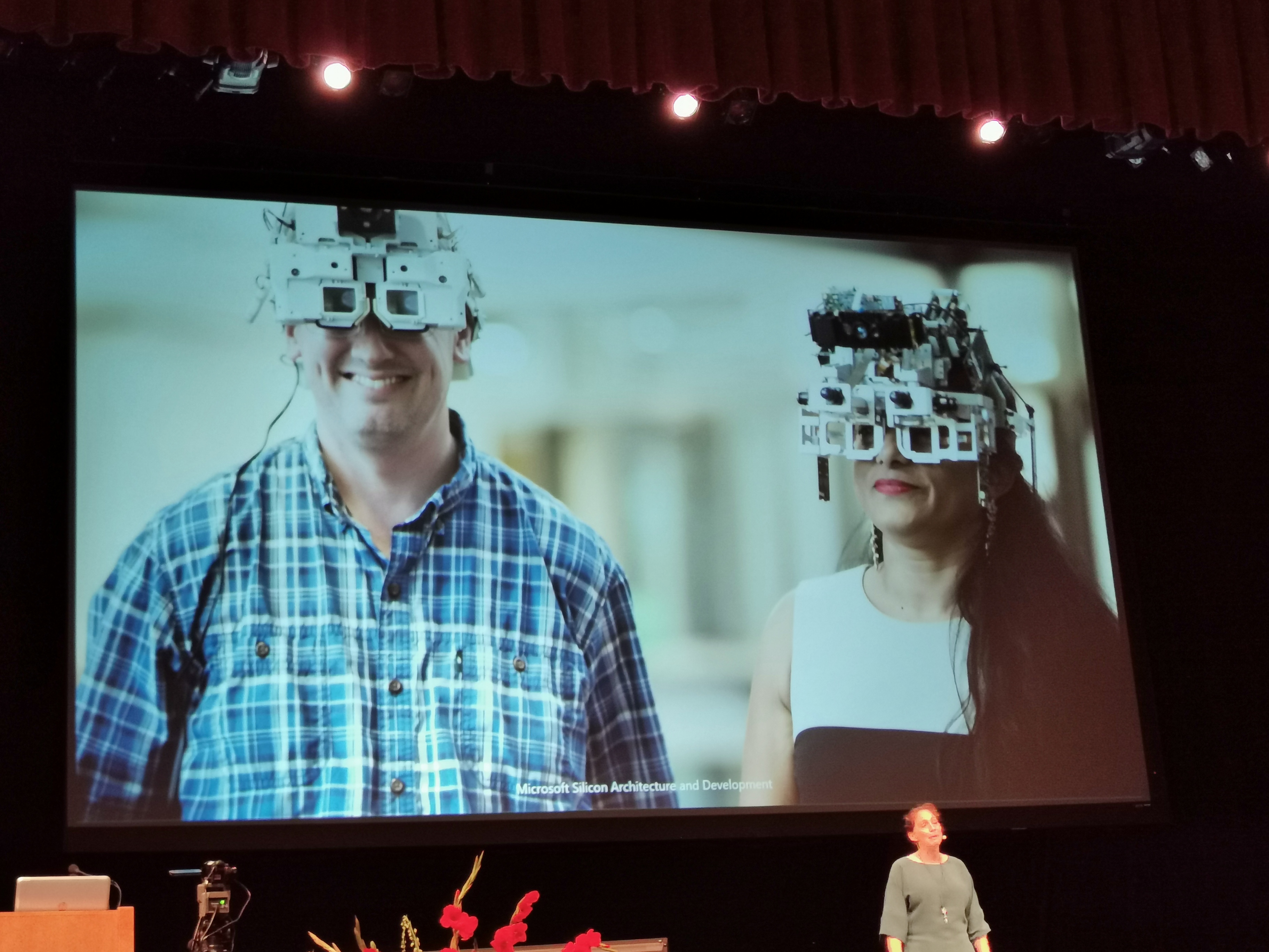
09:22PM EDT – First prototype
09:22PM EDT – First prototype headset*
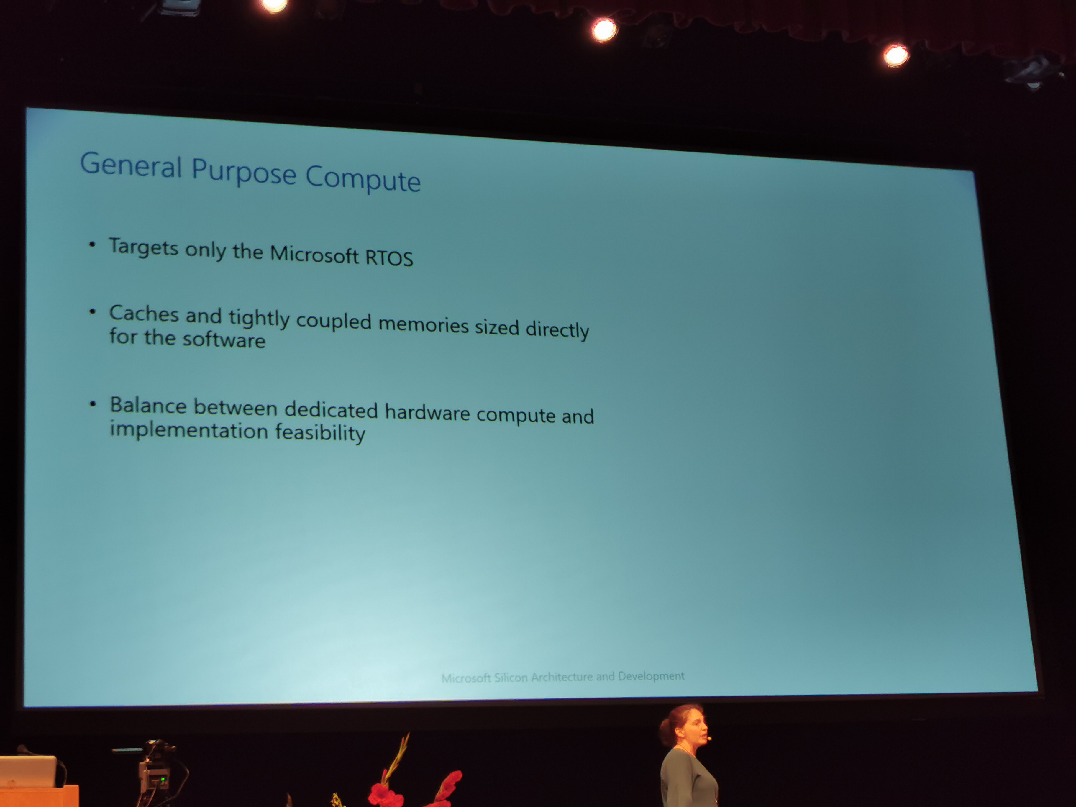
09:23PM EDT – HPU 2 is dedicated to only Microsoft workloads
09:23PM EDT – Targets a single Microsoft RTOS
09:23PM EDT – No MMUs, simple interrupts
09:23PM EDT – Frees up the hardware
09:23PM EDT – Works with the software team to configure caches and memory
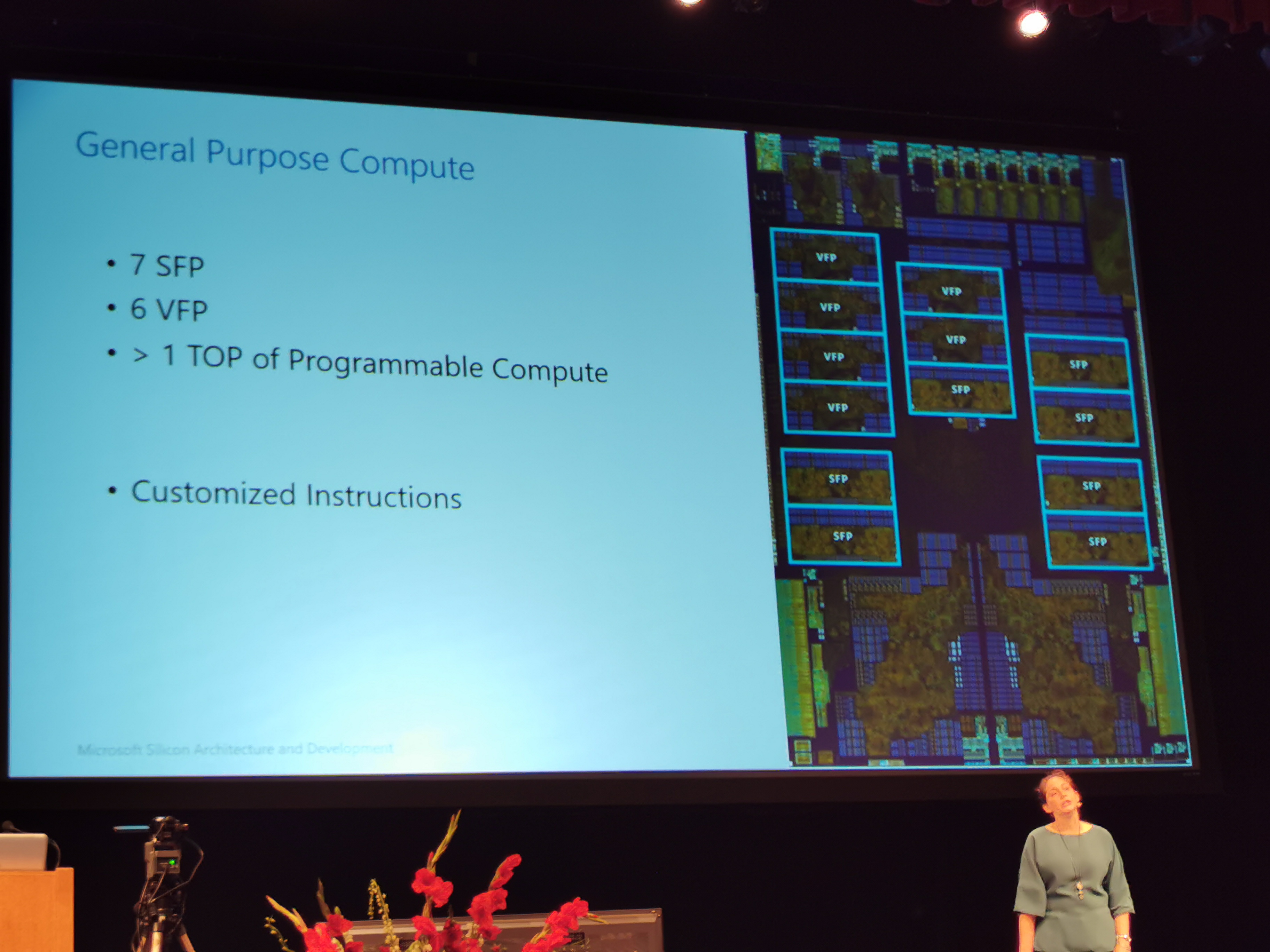
09:24PM EDT – Balance between dedicated HW compute and flexibility / programmability
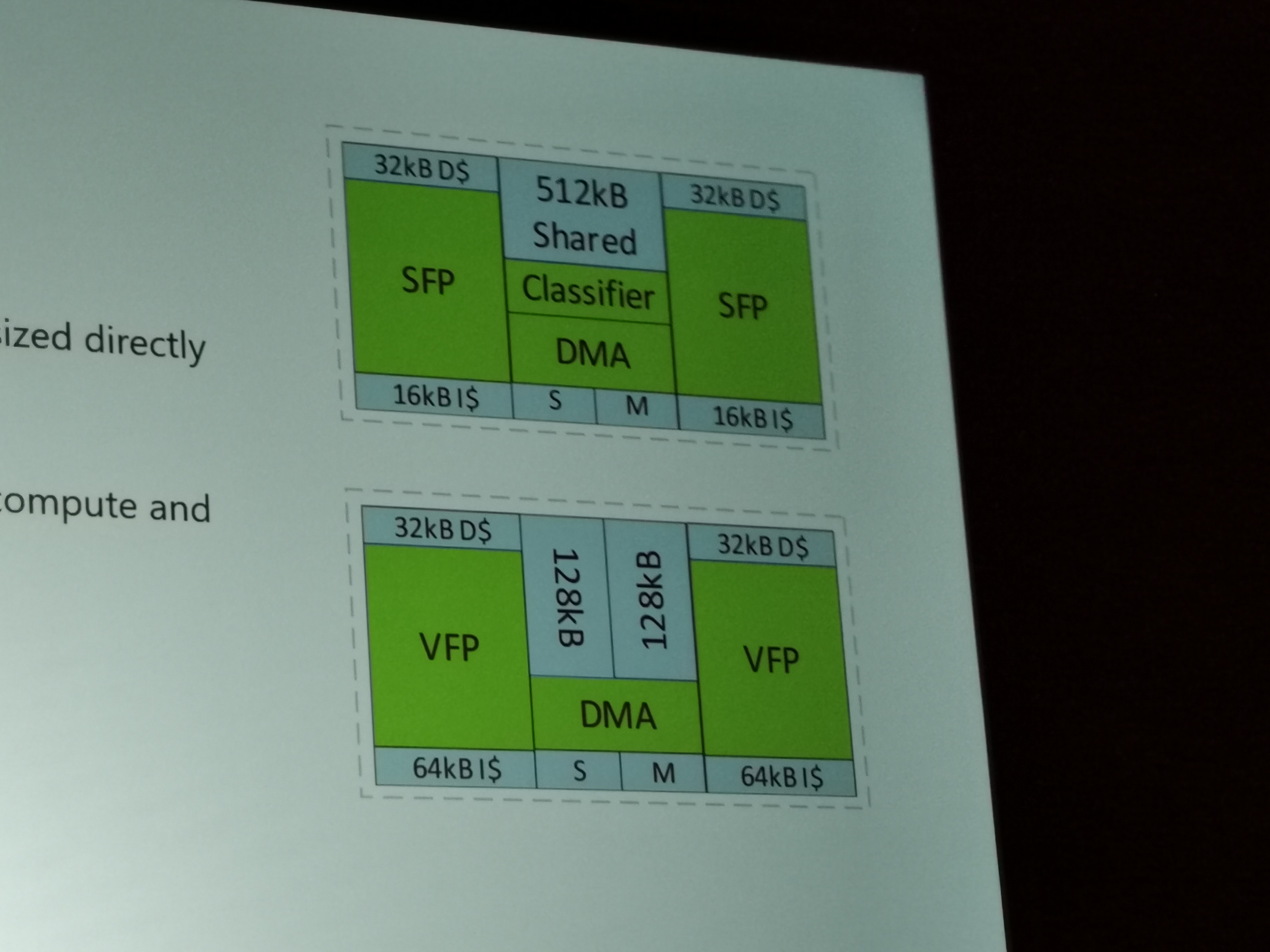
09:24PM EDT – SIMD Fixed Point at top
09:24PM EDT – Does 2D processing
09:24PM EDT – FVP, Floating Vector Processor on bottom, does 3D
09:24PM EDT – 2 Tensiilica processors per node
09:24PM EDT – Trade off area for latency – low latency was key
09:24PM EDT – DMA channel per core
09:25PM EDT – New depth based algorithms

09:25PM EDT – 13 statically assigned compute cores
09:25PM EDT – >1 TOP of programmable compute
09:25PM EDT – 100s of customized instructions
09:26PM EDT – Algorithm profiling to turn 10s of ops into a single instruction
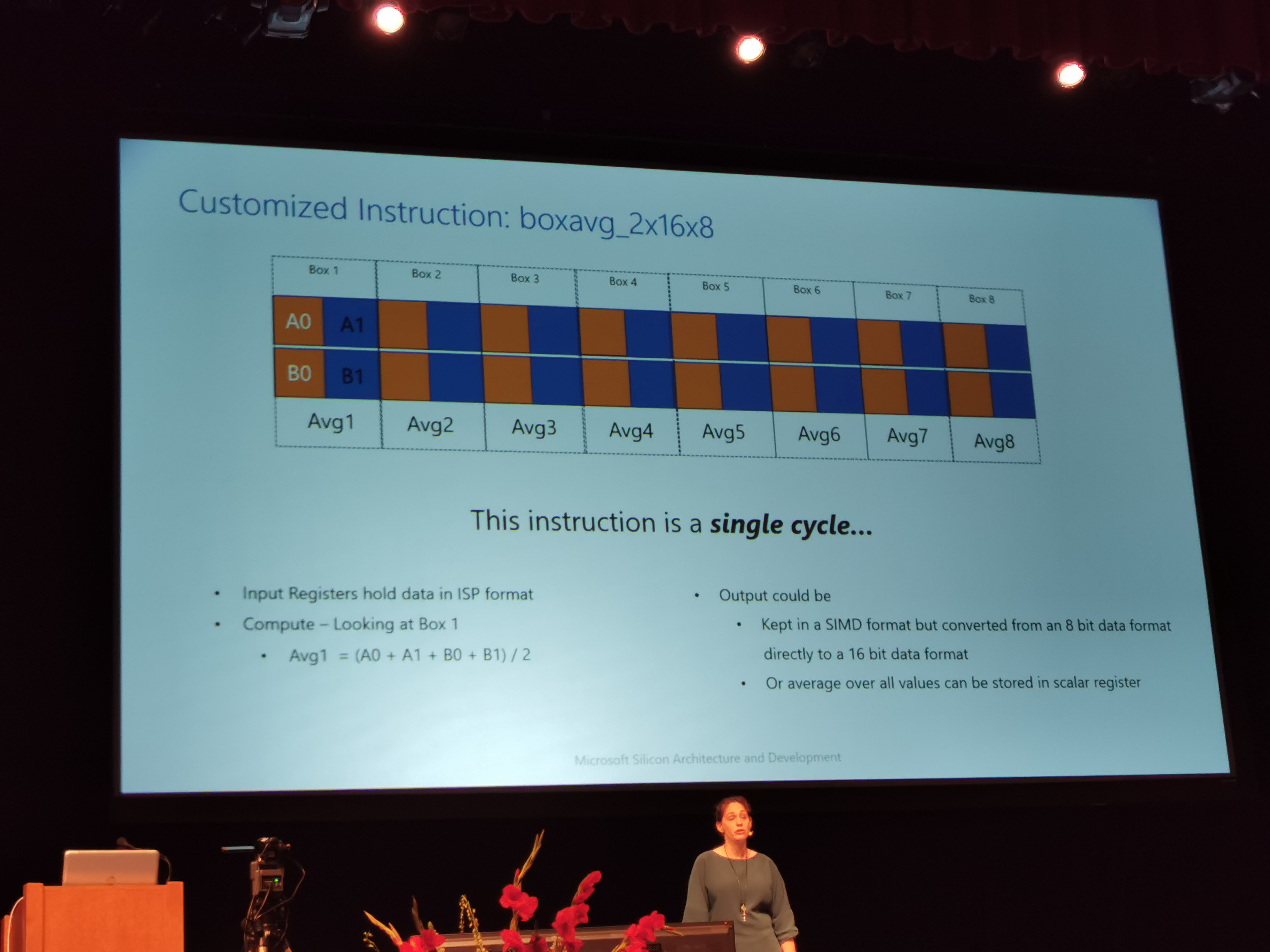
09:27PM EDT – Example, boxavg_2x16x8 is a single cycle instruction
09:27PM EDT – instruction is applied to every pixel, saving 10k+ cycles per frame
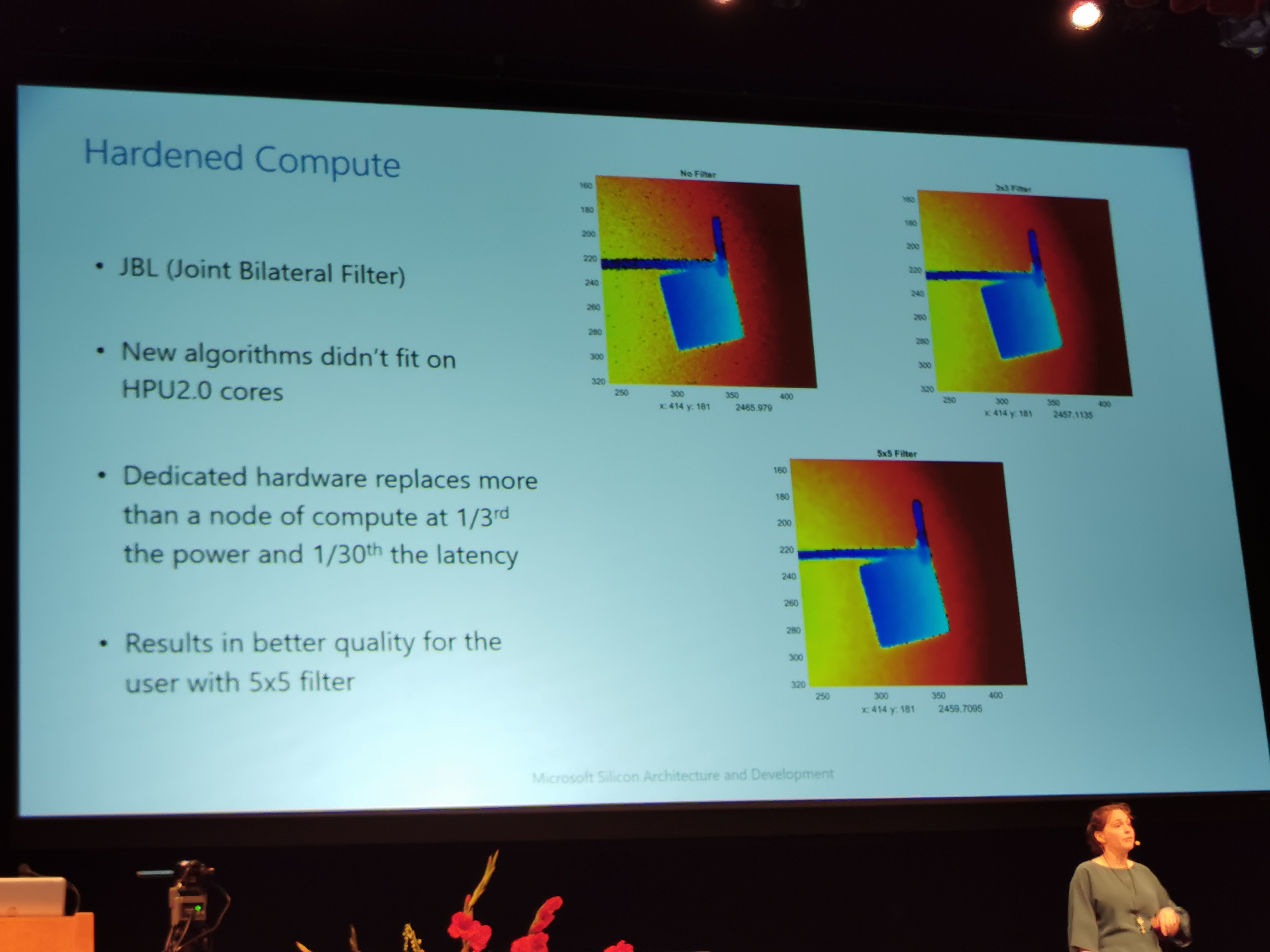
09:27PM EDT – Hardened compute on ToF sensor
09:27PM EDT – JBL filter
09:28PM EDT – Uses 3 sensors and applies filter
09:28PM EDT – But didn’t fit on the node. But adjusted a C model into RTL, for hardware. Reduces power to 1/3, and 1/30th latency
09:29PM EDT – Now thermals
09:30PM EDT – Power gating, clock gating, removing ULV cells
09:31PM EDT – Most digital logic at 250 MHz, compute at 500 MHz
09:31PM EDT – Reduced voltage, Vmin
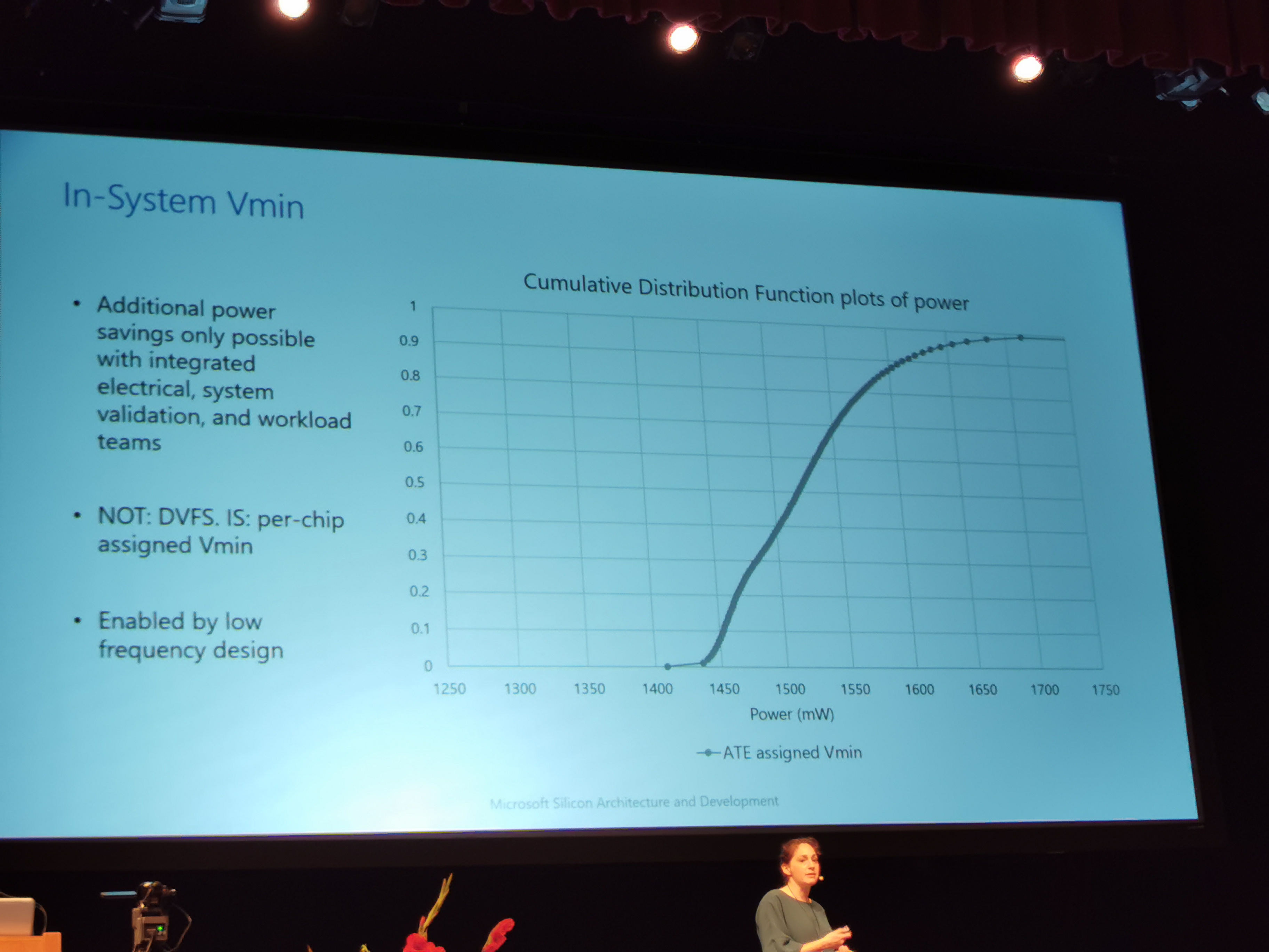
09:31PM EDT – DVFS per chip
09:32PM EDT – Could take the guard bands off
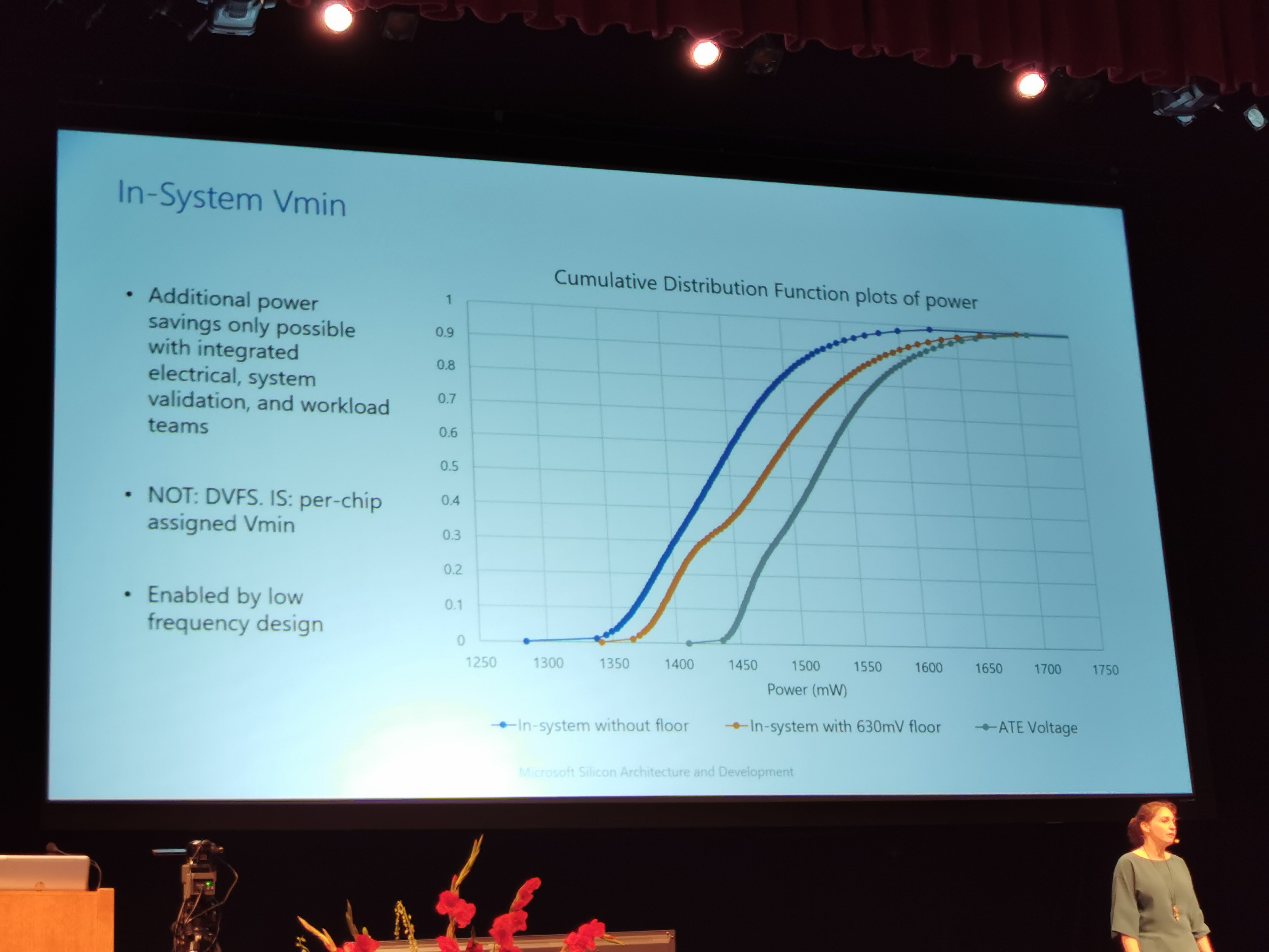
09:32PM EDT – Can reduce the power by 20%
09:32PM EDT – at Vmin
09:32PM EDT – Now system integration
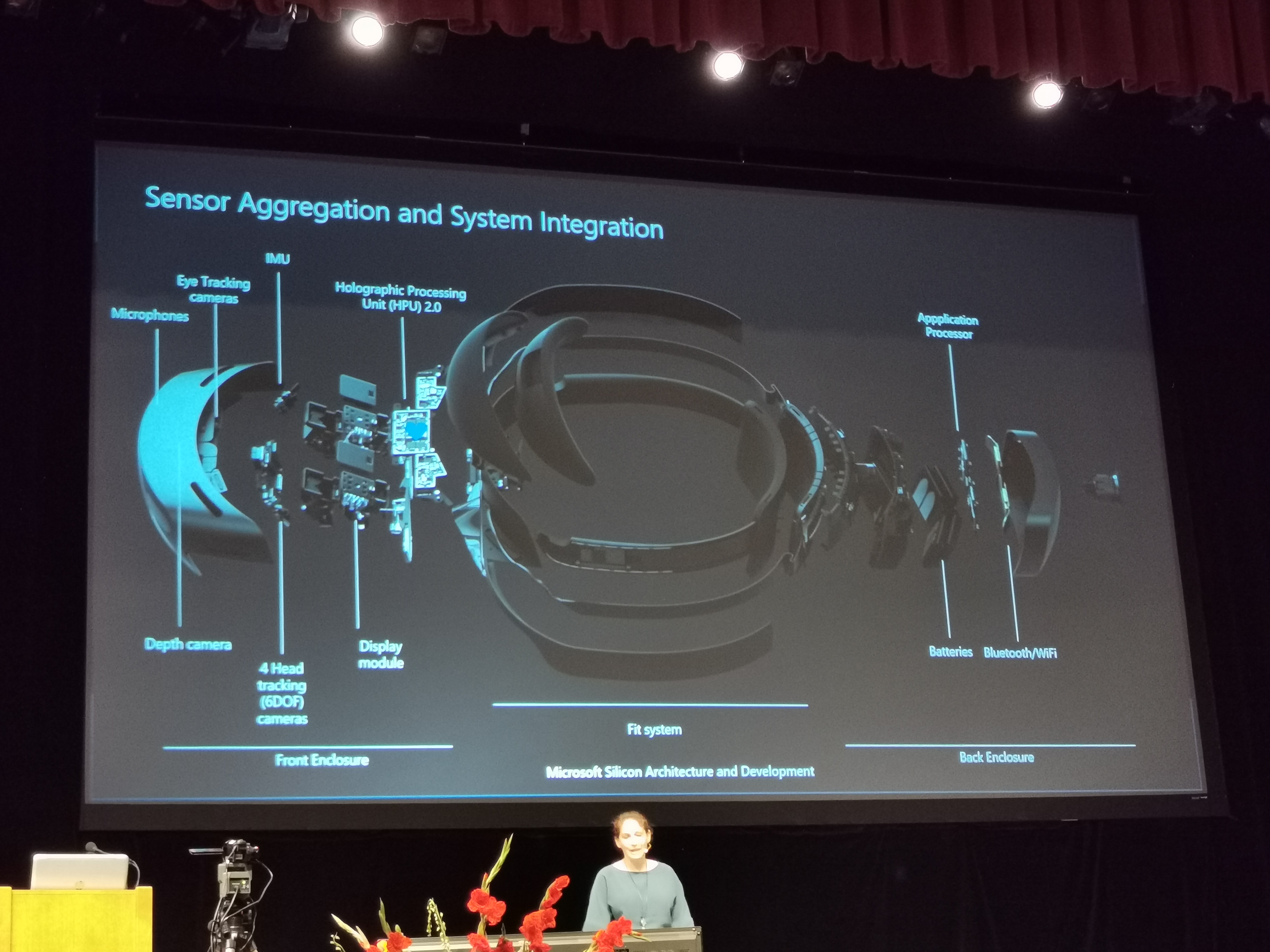

09:33PM EDT – HPU in front, App processor in back
09:33PM EDT – PCIe 2.0 x1 at 100 MB/s comms between front and back
09:34PM EDT – Rendered images sent back via MIPI to HPU
09:34PM EDT – MIPI QoS rates
09:35PM EDT – 6.8 GB/s needed to sync into two lanes of LPDDR4
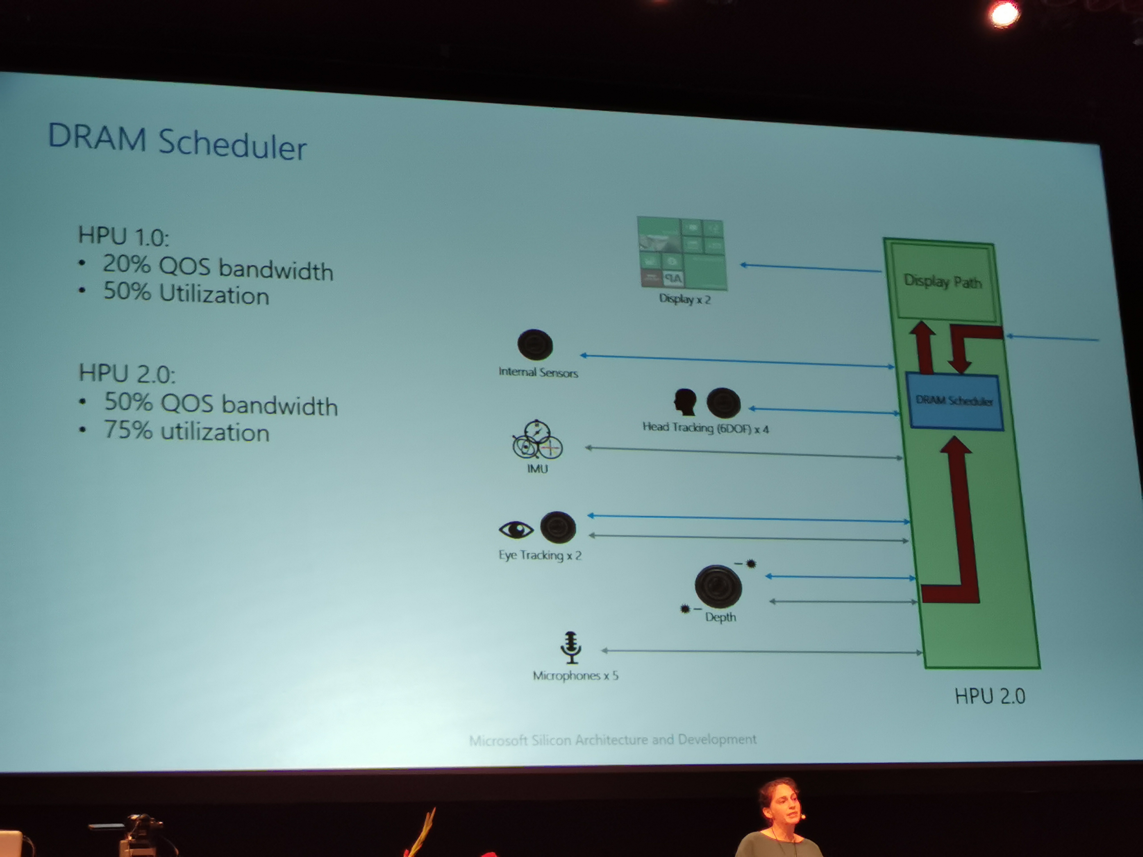
09:35PM EDT – Custom DRAM scheduler on HPU 2.0
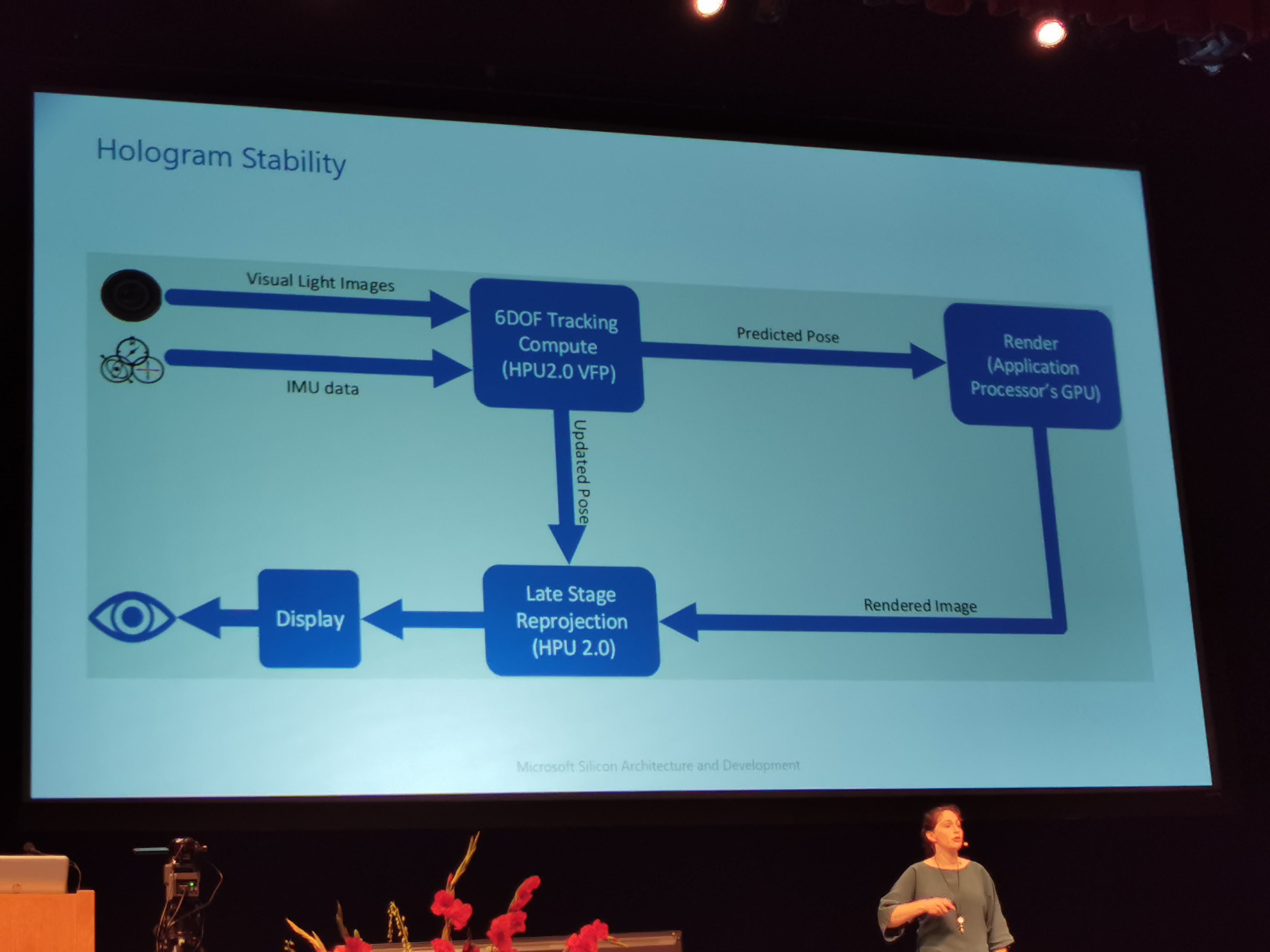
09:36PM EDT – Hologram stability
09:37PM EDT – Multiple pose updates per frame
09:37PM EDT – Hardened block on HPU decouples the render resolution to display resolution
09:37PM EDT – Gives more thermal headroom to GPU
09:38PM EDT – HPU Timestamps the sensor data as it comes in
09:38PM EDT – Hardened neural network
09:39PM EDT – Q&A
09:40PM EDT – Q: Comment on depth camera? A: Custom ToF, there’s a lot of literature out.
09:40PM EDT – Q: Scheduler? A: Statically assigned algorithms to the compute units
09:41PM EDT – Q: Transfer data between different VFPs? A: Small amount of bandwidth between VFPs, but mostly between memory.
09:43PM EDT – That’s a wrap! Thank you for staying with us through all the Hot Chips coverage!